In the photovoltaic market, silicon is currently the most widely used material for making solar cells. Silicon solar cells are available in three main types-
- Monocrystalline silicon solar cells,
- Polycrystalline silicon solar cells, and
- Amorphous silicon solar cells.
The fact that the materials are indirect bandgap semiconductors is the first two justifications for why a particular thickness is required when absorbing solar energy. The PN junction requires more silicon raw material to manufacture since it is relatively thick (typically more than 200 microns). A solar panel still has a hefty price tag, and it also generates a lot of silicon waste. A vital and very versatile semiconductor is silicon. For more details see easybom.
Amorphous silicon is a direct bandgap semiconductor with a broad spectrum of light radiation
absorption and a low required thickness. As a result, amorphous silicon can be used to create
extremely thin film solar cells. The full thickness of the light absorption sheet is around 1
micron and the market choose amorphous silicon because of its lower cost and higher
performance.
History of Amorphous Silicon Solar Cells’ Development
After understanding the possible application of doped amorphous silicon thin films in solar cells,
researchers have been researching amorphous silicon solar cells since 1974.
According to Carlson of RCA, who developed amorphous silicon solar cells employing metal-
semiconductor and p-i-n device designs, the conversion efficiency at the time was less than 1%.
1977: Carlson increases the conversion efficiency of amorphous silicon solar cells to 5.5 percent.
In 1978, the Japanese government used integrated amorphous silicon solar cells for the first time.
1980: ECD developed an amorphous silicon solar cell with a conversion efficiency of 6.3% using
a metal-insulator-semiconductor (MIS) structure; a silicon solar cell pocket calculator.
Amorphous silicon solar cells were first used in clocks, chargers, radios, and other products in
1982.
Composite solar cells built on amorphous silicon were first employed as stand-alone power
sources in 1984.
Amorphous silicon solar cells are the most promising type. As a result, its reputation among manufacturers of semiconductor solar cells as a whole is rising. About one-third of the world’s current total solar cell production, measured in terms of electric power, is made up of amorphous silicon solar cells, the majority of which are used for commercial applications.
Solar Cells Made of Amorphous Silicon: Characteristics
Cheap Price
- The silicon material can completely absorb light while using less material. Due to its high light absorption coefficient, amorphous silicon should be one micron thick and a single crystal 200 microns thick.
- The main raw material used in the production of high-purity polysilicon is silane. This gas can be produced inexpensively and in large quantities by the chemical industry. 6%).
- The thickness of crystalline silicon solar cells varies by more than 200 times, from 240 um to 270 um. For large-scale manufacturing, an astoundingly large number of semiconductor grades are required. The cost of silicon wafers accounts for 65–70% of the total cost of a solar cell. In China, one watt. For crystalline silicon solar cells, the cost of silicon material has surpassed RMB22. Amorphous silicon solar cells and other thin-film solar cells are the onl options available in terms of raw material availability when it comes to using sunlight t generate large amounts of electricity for human consumption.
Big-scale production is simple
Due to the core method’s suitability for the creation of a-Si alloy thin films with very broad areas
free of structural flaws, the pn junction and the accompanying laminated structure can only be
generated by altering the gas phase composition or gas flow.
Diversity and adaptability
The device power, output voltage, and output current of thin-film a-Si solar cells are easily
produced and manufactured. As a result, it is simple to create a range of goods that are appropriate for diverse uses. Due to its strong light absorption coefficient and low dark conductance, it can be used to make low-power indoor power sources such as watch batteries, calculator batteries, etc. Because of its superior mechanical properties, the silicon mesh structure of the a-Si film is perfect for application in thin solar cells on flexible substrates. Building-integrated batteries are perfect for the installation of rooftop solar power systems for residences since they may be made utilizing a range of adaptive production techniques.
Since amorphous silicon lacks the periodic atomic arrangement required for crystal formation, it
can avoid the problem of lattice mismatch between the material and the substrate that must be
taken into account in the creation of crystals. It may therefore be applied quickly across a large
area and applied to almost any surface, even inexpensive glass substrates.
Excellent performance
Under the same lighting conditions, amorphous silicon thin-film cells produce 15% more power
annually than single-crystalline silicon cells. Amorphous silicon cells have the highest efficiency-
to-mass ratio (i.e., they are light and efficient), and their ratio is six times higher than that of
monocrystalline cells, which qualifies them for use in future space solar power plants.
Structure of Amorphous Silicon Solar Cells
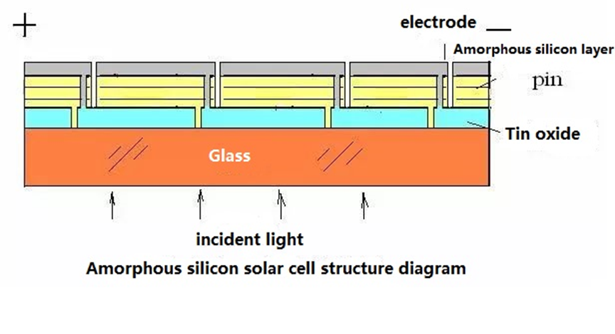
Structure of Amorphous Silicon Solar Cell (Images Source)
Amorphous silicon solar cells often have a p-i-n structure as opposed to monocrystalline silicon solar cells, which typically have a p-n structure. This is because amorphous silicon that has been a little doped has a smaller Fermi level shift, therefore using a material that has been weakly doped on one side and highly doped on the other will result in less band bending. Because of the higher density of defect states in the extensively doped amorphous silicon material, the minority carrier lifetime is low when the p+-n+ junction is constructed directly using severely doped p+ and n+ materials, which lowers battery performance. a terrible notion. In order to create the active collector region, a layer of amorphous silicon that is undoped is frequently deposited in between the two layers that are highly doped.
In amorphous silicon solar cells, photogenerated carriers are largely generated in the undoped i layer, as opposed to crystalline silicon solar cells, where photogenerated carriers migrate primarily due to diffusion. In this cell, the drift motion of photogenerated carriers is essentially governed by the electric field of the solar cell.
In amorphous silicon solar cells, the top, the heavily doped layer is thin and practically transparent, allowing incident light to flow through and generate free photogenerated electrons and holes in the undoped layer. From this point, the higher built-in electric field also expands substantially, and the photogenerated carriers are quickly swept to the n+ and p+ sides after being created.
Undoped amorphous silicon is essentially a weak n-type material; however, by introducing a trace amount of boron during the active collector zone deposition, it can be converted into an i-type with the Fermi level centered. This increases the amount of solar energy. battery performance The deposition sequence is often set up as p-i-n during the actual preparation process to guarantee that the active collector region is naturally doped with boron when the p-layer is created. According to this deposition order, the opaque substrate cell will always face the n+ layer, whereas the transparent conductive substrate cell will always face the p+ layer.
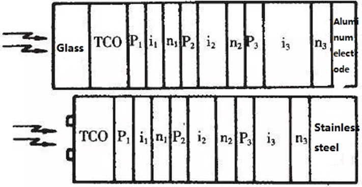
Amorphous silicon tandem cells Even when composed of crystalline materials, single-junction solar cells have a theoretical maximum conversion efficiency of just about 25% when exposed to AM1.5 light. This is so because a semiconductor can only absorb photons whose energy is greater than the value of its own band gap, and the solar spectrum’s energy distribution is relatively wide. The remaining photons either pass through the battery and are absorbed by the metal on the back and converted to heat, or they pass through the battery and transfer energy to the atoms of the battery material itself, causing the material to heat up. None of this energy can be converted into electricity by creating photogenerated carriers. Additionally, the thermal effect of these photons might worsen battery performance by raising the operating temperature of the battery. to maximize the efficiency of solar energy over a wider range of wavelengths. People divide the solar spectrum into numerous portions and select materials whose energy gaps are best matched to these regions in order to produce cells with a spectral response that is close to that of sunlight. As seen in the figure, a solar cell with this form of structure is referred to as a layered battery.
Amorphous Silicon Solar Cell (Images Source)
Production of Amorphous Silicon Thin Film Solar Cells and Manufacturing Methods
Amorphous silicon thin-film solar cells are primarily produced using the following machinery:
large-scale amorphous silicon thin film PECVD production machinery, infrared and green laser engraving machinery, large magnetron sputtering production machinery, and component testing machinery.
- Chamfering: Take special care to chamfer the eight edges of the clear conductive glass and to round out any sharp corners.
- Thoroughly washing and drying the transparent, double-sided, conductive glass surface.
- Laser-engrave lines on the transparent conductive glass, reserve a certain number of substrates, and check the resistance with a multimeter to be greater than 1M (megaohm); in production, we use 20K. The measurement was performed using the conductive film (double junction product; there are 39 cells and a 15.5mm sub-cell spacing).
- Secondary cleaning, including thorough wiping, drying, and cleaning the transparent conductive glass surface.
- Loading: Place the conductive glass inside the workpiece’s frame so that it may be heated up and coated. During the loading process, you must take care to prevent the conductive glass film surface from reversing.
- Preheating: Ensure that the conductive glass is heated uniformly and to the temperature required for PECVD deposition (215°C in the preheating furnace).
- PECVD: A large, uniform PIN layer is deposited to the conductive glass while it is under
vacuum. After deposition, the battery chip doesn’t have any obvious chromatic aberration or stripes. There are no obvious pinhole occurrences when a flashlight is shone on the battery chip. - Cooling (unloading): The glass is unloaded after cooling in the workpiece rack. High temperatures should not be used to put glass onto the workpiece rack since doing so could cause it to flex or break.
- To create a conductive channel for attaching the sub-battery, use a 532 green laser to scribe lines on the partially finished chip where the silicon layer has been applied. The laser spot is consistent, clean, and smooth; it cannot be rounded, crooked, or have burrs.
- PVD (magnetron sputtering): The resistance of the back electrode is less than 10 ohms, the back electrode (AL or AZO+AL) is plated, and the battery chip does not peel after aluminum plating.
- Laser scribing in threes uses an aluminized back electrode to draw lines on the partially finished chip to finalize the series connection of the sub-cells.
- Clear the 10mm space along the chip’s four borders to reach the insulation condition.
- Annealing: Recombining the microstructure of the thin film material through heat treatment to boost its stability can improve the conversion efficiency of the battery chip.
- Check: Examine the electrical specs of the battery chip.
- Back-pressure: Back-pressure improves a chip’s conversion efficiency by addressing its
shortcomings.
The manufacturing process for amorphous silicon thin film solar cells is the quickest of all photovoltaic cells. However, the specifications for vacuum PECVD manufacture of amorphous
silicon semiconductor films are quite strict, from film design through process control. While the large-area modules produced by the method have not yet reached the permitted efficiency of 6% on most manufacturing lines, the small-area cells now prepared in laboratories have an efficiency of about 15% for photoelectric conversion. The theoretical limit of large-area components is 85% to 90% of that of small-area components. The variance in photoelectric conversion efficiency between small-area components and other components indicates the technical competence of a production line.
Only a few amorphous silicon production lines worldwide have produced modules with a certified efficiency of more than 8% due to the performance of nearly all other types of photovoltaic modules (including the currently contentious microcrystalline silicon thin-film cells) in actual operating conditions of high-temperature, cloudy days, and low illumination. The fact that amorphous silicon modules perform so well under these real-world operating circumstances has allowed several kinds of large-area thin-film cells to produce modules with certified photoelectric conversion efficiencies of over 12% in the past, even on a huge scale. Amorphous silicon photovoltaic modules cannot be disregarded for power generation applications due to their lowest manufacturing costs, moderate, and not as poor as falsely reported photoelectric conversion efficiency, as well as their beautiful translucent modules, bendable, high-quality Light, and unbreakable flexible components, and other applications that only have the superior performance of amorphous silicon.
Effect of Photodegradation On Amorphous Silicon Material Flaws
The hydrogen-doped amorphous silicon thin films used in solar cells have a significant drawback called the light-induced degradation effect. When the hydrogenated amorphous silicon film is subjected to strong light or current for a lengthy period of time, H is quickly lost and a considerable number of Si dangling bonds are generated, lowering the electrical properties of the film. This is because the Si-H bond is weak (bond energy 323). This loss of H behavior also causes a chain reaction because the H atom on the adjoining bond is drawn to the dangling bond of the lost H, which loosens the Si-H bond around it and causes the nearby H atom to combine into H2, which (H-H bond energy 436) makes it simpler to create H2 bubbles. The photoelectric conversion efficiency, which will decrease as illumination time increases, will have a substantial impact on the performance of solar cells. Due to the material’s weak response to long-wavelength solar light due to its optical band gap of 1.7 eV, amorphous silicon solar cells have a low conversion efficiency.
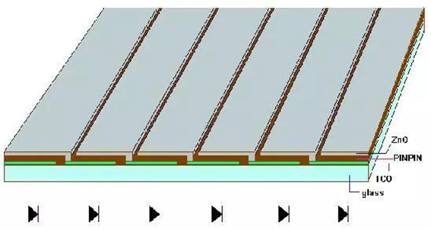
A multi-level solar cell group can be created by wiring many batteries in series in order to prevent the weakening of the absorption of incident light caused by the thinning of the thickness. As a result, the battery’s i-layer thickness can be reduced. absorb. Tandem solar cells are built-up versions of one or more p-i-n single junction solar cells.
Amorphous Silicon Solar Cell (Images Source)
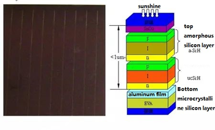
As depicted in the diagram above, one PIN junction is placed on top of another. The concept behind tandem amorphous silicon solar cells is that because to the wide energy distribution in the solar spectrum, any existing semiconductor material can only absorb photons whose energy is higher than its energy gap value. Less powerful solar photons will enter the battery, be absorbed by the metal of the back electrode, and be converted into heat energy. The pyrolysis of photogenerated carriers, on the other hand, will allow high-energy photons with energies greater than the energy gap width to transmit their energy to the battery material itself. The atoms in the material’s lattice structure cause the material to heat up directly. None of these energies can be transported to the load by photogenerated carriers and turned into usable electrical energy. Therefore, even if single-junction solar cells are made of crystalline materials, their theoretical maximum conversion efficiency is typically just around 25%. The battery should be made of a material that has the best energy bandwidth match for each of the parts of the sunlight spectrum, and it should be superimposed from the outside to the inside in the order of the energy gap from the largest to the smallest. The outermost wide-gap material cell uses the light, and the longer wavelength light can be transmitted into and used by the narrower energy-gap material cell in order to enhance the conversion of light energy into electrical energy. One example of this type of cell structure is laminated cells.
Other batteries lack the ability to restore efficiency to 80%-97% of the original value after annealing at 130-175 degrees Celsius in amorphous silicon cells with reduced conversion efficiency caused by photo-induced degradation, in which the H-H bond is broken and the Si-H bond is re-formed.
Amorphous Silicon Cell Performance Influencing Factors and Development Prospects
The amorphous silicon structure’s long-range disordered random network topology greatly scatters the carriers, making it ineffective at efficiently gathering them. The conversion efficiency and stability of amorphous silicon solar cells are typically not improved by the monocrystalline silicon solar cells’ p-n structure. This is true because to the little Fermi level change in amorphous silicon with mild doping. If both sides are mildly doped or if one side is weakly and the other heavily doped, the energy band bending will be reduced and the battery’s open circuit voltage will alter. Limitation; If the p+-n+ junction is made directly utilizing extremely doped p+ and n+ materials, the cell performance will be poor due to the high density of defect states and short minority carrier lifetime in the severely doped amorphous silicon material. An undoped amorphous silicon layer (i-layer) is often sandwiched between two substantially doped layers to produce a p-i-n structure.
In amorphous silicon solar cells, photogenerated carriers are largely generated in the undoped i-layer as opposed to crystalline silicon solar cells, where carriers migrate primarily due to diffusion. The small’s drift movement is primarily caused by the electric field of the battery. Although an amorphous silicon battery with a pin structure can function in the presence of light, its performance is unstable and its conversion efficiency gradually declines over time due to the effect of light-induced degradation. The battery’s structure and manufacturing procedure must therefore be improved.
The main factors affecting the conversion efficiency and stability of amorphous silicon cells are
transparent conductive film, window layer characteristics (such as optical band gap width, conductivity, and doping concentration), window layer activation energy, and window layer light
transmittance. Overrate), the energy gap matching, the density of the interface defect state, the
thickness of each layer (especially the thickness of the I layer), and the solar cell’s architecture,
among other things. Typically, heterojunctions that have been integrated, stacked, or otherwise
constructed make up amorphous silicon thin-film cells.
The market share of amorphous silicon cells is increasing every year due to its simple production process, which requires little heat and energy. More than half of thin-film solar cell companies presently employ amorphous silicon thin-film technology, and it is projected that within a few years, amorphous silicon thin-film will account for a sizeable portion of future thin-film solar cells. However, low photoelectric conversion efficiency and light-induced degradation are the two fundamental problems with current amorphous silicon thin-film cells. In order to improve efficiency and stability, researchers must step up their investigation of novel device structures, novel materials, novel processes, and novel technologies.
For instance, stacked and integrated battery structures are employed; in the field of transparent
conductive films, the current ITO, ZnO, ZnO#Al, and other conductive films are replaced with a
a transparent conductive film that not only has low resistivity but also has the ability to block ion
pollution, increase incident light absorption, and have anti-radiation properties; Investigate new
window layer materials, such as amorphous silicon carbon, amorphous silicon oxygen, microcrystalline silicon, and microcrystalline silicon carbon, have a broad optical band gap and low resistance; The carrier transport capability, electron density, and photon life of the amorphous silicon film can be improved using the RF-PECVD, ultra-high vacuum PECVD, very high frequency (VHF) PECVD, and microwave PECVD methods of film formation. Buffer layer insertion and hydrogen passivation technology are two interface treatment methods that can be used to improve battery short-circuit current and open-circuit voltage while reducing interface recombination loss. Amorphous silicon thin film solar cells’ poor efficiency and inconsistent performance are the main obstacles to their widespread industrial manufacturing, however, there are still many ways to make them more effective. The use of thin-film solar cells will be commonplace.
Read the article related to solar systems:
- Best Solar Panel
- Uses of Solar Energy
- Benefits of Solar System
- Solar Inverter vs. Power Inverter
- On-Grid vs Off-Grid Solar Systems
- Top 10 Solar Power Plants
- Automatic Solar Tracking System Project
Thanks for Reading